3When poly crosses diffusion it represents a transistor. Valerio Re - INFN.
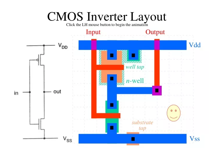
Ppt Cmos Inverter Layout Powerpoint Presentation Free Download Id 9289699
Gate-level mux design how many transistors are needed.

. 3 Design Rules CMOS VLSI Design Slide 5 Feature Size Feature size improves 30 every 2 years or so 12 07 reduction factor every generation from 1 μm 1000 nm in 1990 to 14 nm in 2015. Cross-Section of CMOS Technology Design Rules Interface between designer and process engineer Guidelines for constructing process masks Unit dimension. The MOSIS design rules are as.
INFN WP3 CMOS ASICs for 3D. 20 transmission gate mux nonrestoring mux uses two transmission gates transmission gate mux nonrestoring mux uses two transmission gates only 4 transistors inverting mux inverting multiplexer use compound aoi22 or pair of tristate inverters essentially the same thing noninverting. 4In CMOS a demarcation line is drawn to avoid touching of p-diffusion n- diffusion.
Design Rules Design rules are a set of geometrical specifications that dictate the design of the layout masks A design rule set provides numerical values For minimum dimensions For minimum line spacings Design rules must be followed to insure functional structures on the fabricated chip Design rules change with technological. When the gate is at a high voltage. 4 Once the layout is complete then a process called layout versus schematic LVS is applied to determine if the physical layout represents the electrical schematic.
Design Rules Allow for a ready translation of a circuit concept into an actual geometry in silicon Provide a set of guidelines for constructing the fabrication masks Minimum line width Minimum spacing between objects. Rabaey Cross-Section of CMOS Technology Design Rules Interface between designer and process engineer Guidelines for constructing process masks Unit dimension. PowerPoint PPT presentation.
Department of Electrical Engineering National Central University Jhongli Taiwan. WP3 AIDA meeting CERN February 16 2011. Simple for the designer.
20 transmission gate mux nonrestoring mux uses two transmission gates transmission gate mux nonrestoring mux uses two transmission gates only 4 transistors inverting mux inverting multiplexer use compound aoi22 or pair of tristate inverters essentially the same thing noninverting. Main objective of design rule is to achieve a high overall yield and reliability using smallest possible Silicon area. 1 Rules for N-well as shown in Figure below.
Ad Download Millions of Presentations Graphic Assets Fonts Icons More. CMOS Layout and Design Rules Continued The most important masks are for the active region and for gate polysilicon. Electrical and Computer Engineering Department.
CMOS lambda Design Rules. 3 During the layout the designer must obey a set of rules called design rules. Gate-level mux design how many transistors are needed.
CMOS λ Design Rules. 10 generations in 20 years 1000 700 500 350 250 180 130 90 65 45 32 22 14 10 nm 0 10 20 30 40 50 60 70 80 90 2005 2010 2015 2020 2025 2030. Advanced Reliable Systems ARES Lab.
I They guarantee that the transfers onto the wafer preserve the topology and geometry of the patterns. The design rules for the layout transistors are often expressed in terms of 2P. Minimum separations minimum and maximum widths overlap rules.
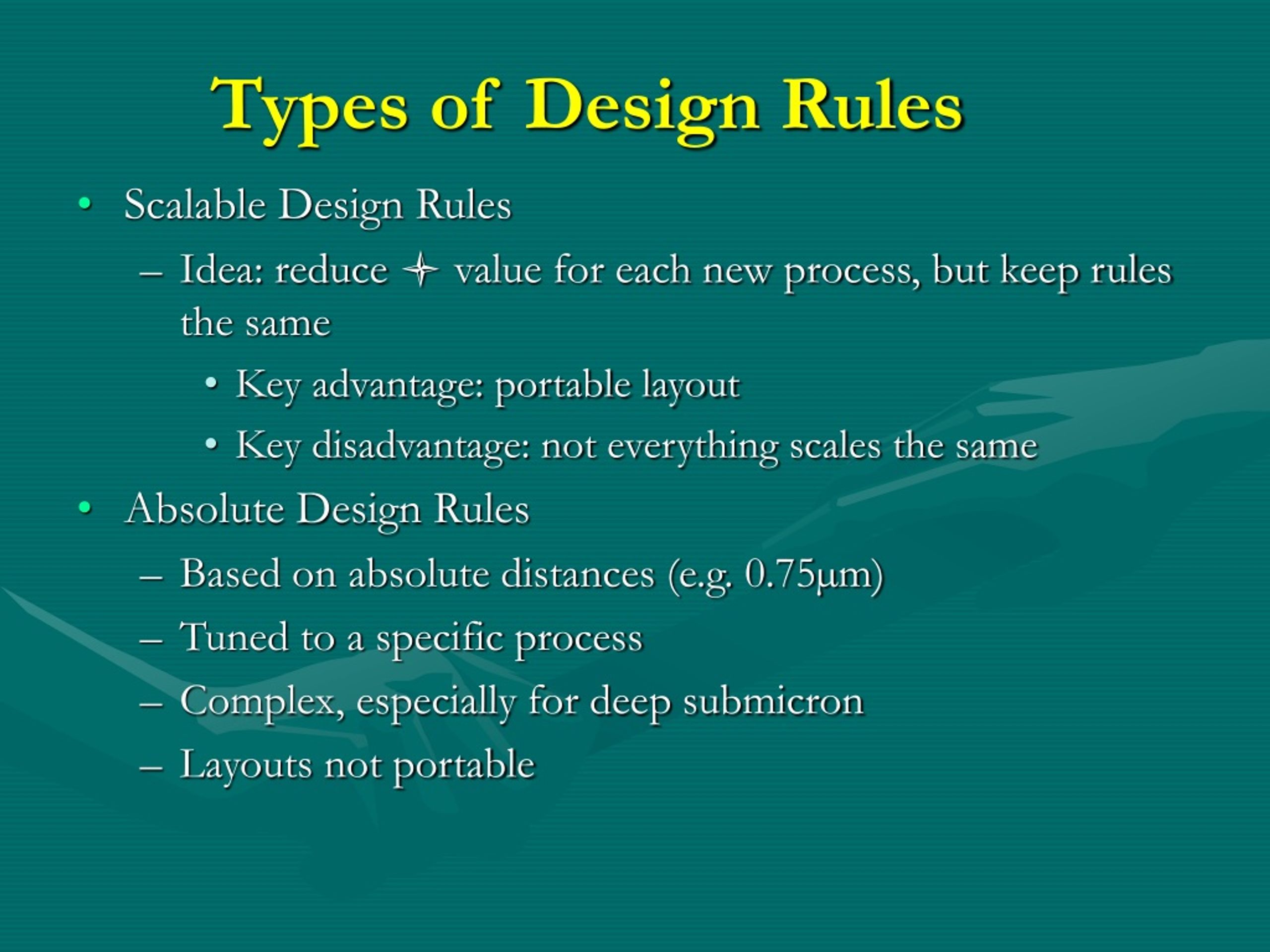
Define cmos design rules presentation slideshows. Advanced Reliable Systems ARES Lab. CMOS VLSI DESIGN LAMBDA BASED DESIGN RULES The design rules may change from foundry to foundry or for different technologies.
Lambda Based Design Rules. INFN WP3 CMOS ASICs for 3D. Must have exactlya fixed size.
From WP3 description. 2P is the minimum technology gate length. The MOSIS rules are scalable λ rules.
IThegeometric design rulesare a contract between the foundry and the designer. Lambda parameter absolute dimensions micron rules CMOS Process Layers Intra-Layer Design Rules Transistor Layout Vias and Contacts Select. All p-MOS should lie on one side of the line all n-MOS should be on the other side of the line.
Spacing Width Notch Kerbe between same net Finest structure is Poly-silicon for gates Some structures have rules ie. The MOSIS stands for MOS Implementation Service is the IC fabrication service available to universities for layout simulation and test the completed designs. Layout Design Rules Introduction Physical mask layout of any circuit to be manufactured using a particular process must follow a set of rules.
VLSI Systems Design Design Rules for CMOS Lecture 7. Design Rules Jan M. Introduction to CMOS Circuit Design Jin-Fu Li Advanced Reliable Systems ARES Lab.
Design rules based on single parameter λ. Positive charge on gate of mos capacitor negative charge is attracted to body under the gate inverts a channel under gate to n-type n-channel hence called the nmos if the gate voltage is above a threshold voltage vt now current can flow through n-type silicon from source through channel to drain. AGH-UST CERN CEA CNRS-CPPM CNRS-LAL CNRS-IPHC INFN-Pavia.
Cross-Section of CMOS Technology Design Rules Interface between designer and process engineer Guidelines for constructing process masks Unit dimension. 3 Must be wide enough to enclose a contact. University of Puerto Rico at Mayagüez.
The interaction of these two masks becomes the channel. The rules define minimum wire widths to avoid breaks minimum spacing to avoid shorts between neighboring wires and minimum overlap to minimize parasitic capacitance. Minimum line width scalable design rules.
18 Circuits-C CMOS VLSI Design Slide 35 Race Condition Back-to-back flops can malfunction from clock skew Second flip-flop fires late Sees first flip-flop change and captures its result Called hold-time failure or race condition CLK1 D Flop Q1 Flop CLK2 Q2 CLK1 CLK2 Q1 Q2 Circuits-C CMOS VLSI Design Slide 36 Nonoverlapping Clocks Nonoverlapping clocks can. DESIGNRULES Rules in one Layer Caused by manufacturing limits lithography etching Rules. 3when poly crosses diffusion it represents a transistor.
Combinational circuit design layout. Access to full CMOS wafers WP3 participants. Cmos design rules the physical mask layout of any circuit to be manufactured using a.
So to make the design rules generic the sizes separations and overlap are given in terms of numbers of lambda λ. IThese rules are the designers interface to the fabrication process. Jin-Fu Li EE NCU 2 Introduction MOS Transistor Switches CMOS Logic Circuit and System Representation Outline.
The actual size is found by multiplying the number by the value for lambda for that specific foundry. IThey guarantee that the transfers onto the wafer preserve the topology and geometry of the patterns. 1 vlsi design cmos layout 2 cmos layout layout design rules describe how small features can be and how closely they can be reliably packed in a particular.
They usually specify min allowable line widths for physical object on chip. Define cmos design rules - PowerPoint PPT Presentation. Cmos design rules the physical mask layout of any circuit to be manufactured using a.
The MOSIS design rules are as follows. These rules are for the purpose of ensuring the robustness and reliability of the technology.
Vlsi Design Cmos Layout Ppt Download
Computer System Computer System System Problem Solving

102737180 Layout Design Rule Ppt Vlsi Design And Layout Practice Lect5 Stick Diagram Scalable Design Rules 108 05 02 1 Ic Layout Concept And Course Hero

Introduction To Cmos Vlsi Design Lecture 1 Circuits Layout Lecture Design Rules Dry Erase Markers
Cmos Design Rule

Ppt Cmos Vlsi Design Powerpoint Presentation Free Download Id 228555
Ppt Layout Design Rules Powerpoint Presentation Free Download Id 9170183

The Cmos Vlsi Design
0 comments
Post a Comment